The same matrix multiply runs 100× faster on one chip than another. This is why, told from the silicon up, with diagrams, for people who train and serve models.
Contents
- Why Different Chips Exist
- CPU vs GPU vs TPU: The Fundamental Divide
- How Each One Runs Work
- Tensor Cores & Matrix Engines
- GPU Memory: HBM, VRAM, Bandwidth
- Talking Between Chips: Communication
- When to Use Each
- It All Happens in One Training Step
- Cheat Sheet
- References
1. Why Different Chips Exist
All three chips are built from the same transistors. The difference is what those transistors are spent on, and that choice follows from one question: are you optimizing for latency, throughput, or a single operation?
- A CPU spends most of its silicon on control and cache so a single stream of instructions finishes as fast as possible. It optimizes latency.
- A GPU spends silicon on arithmetic units instead, thousands of them. Each is slow, but memory stalls on one are hidden by switching to another. It optimizes throughput.
- A TPU spends silicon on one giant matrix-multiply unit, trading away flexibility to do deep learning's dominant operation as efficiently as physics allows. It optimizes a single kernel.
🧠 CPU
A few powerful, clever cores. Wins on serial, branchy, latency-sensitive work.
🎛️ GPU
Thousands of simple cores running together. Wins on data-parallel throughput.
⚙️ TPU
An ASIC built around a matrix engine. Wins on large, dense matrix math.
The clearest way to feel the difference is to watch the same work flow through each chip: one item at a time, thousands at once, or streaming through a grid:
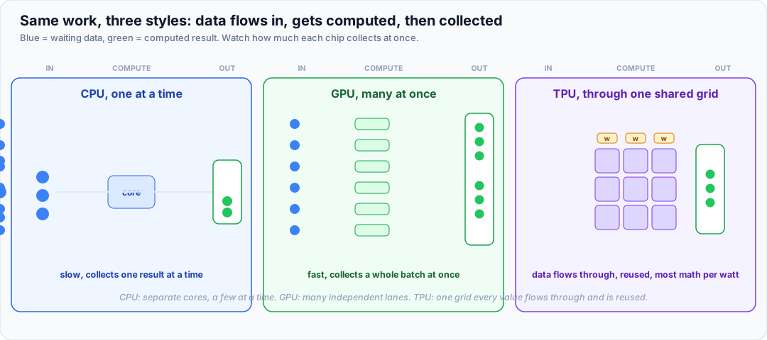
Why this matters for an infra role: when a workload is slow, the first question is which resource it actually spends: control flow, memory bandwidth, or matrix FLOPs. The hardware should match where the work goes. The rest of this piece is about making that judgment precisely.
2. CPU vs GPU vs TPU: The Fundamental Divide
The CPU: a latency machine
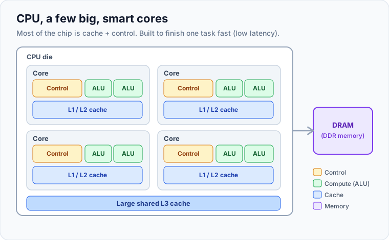
A CPU core is built to finish one instruction stream quickly. It speculatively executes branches, reorders instructions to hide memory latency, and keeps a deep cache hierarchy (L1/L2/L3) close so data is rarely far away. It has only a handful of cores, each with wide SIMD units (AVX-512, ARM SVE) for modest data parallelism. CPUs win when work is irregular: branches, pointer chasing, small data, strict ordering, or latency-sensitive request handling.
The GPU: a throughput machine
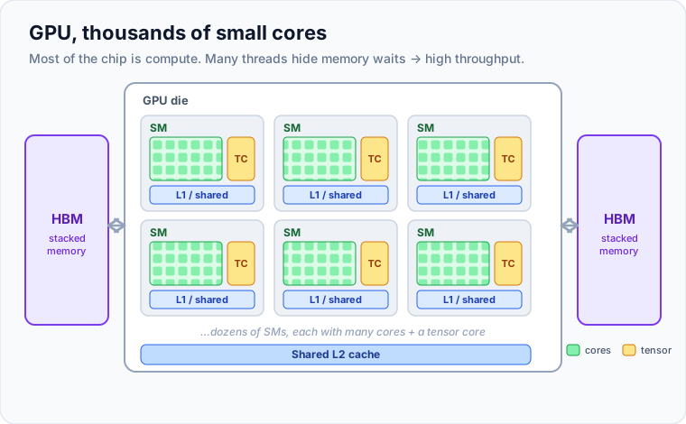
A GPU inverts the priorities. It packs in dozens of Streaming Multiprocessors (SMs), each with many small cores, for tens of thousands of concurrent threads, and surrounds them with very fast HBM memory. Individual threads are slow with almost no per-thread cache, but when one group stalls on memory the SM instantly switches to another that's ready. With enough threads in flight (occupancy), memory latency is hidden rather than avoided. The payoff is huge throughput on regular, parallel work, which is exactly what neural networks are.
The TPU: a specialized machine
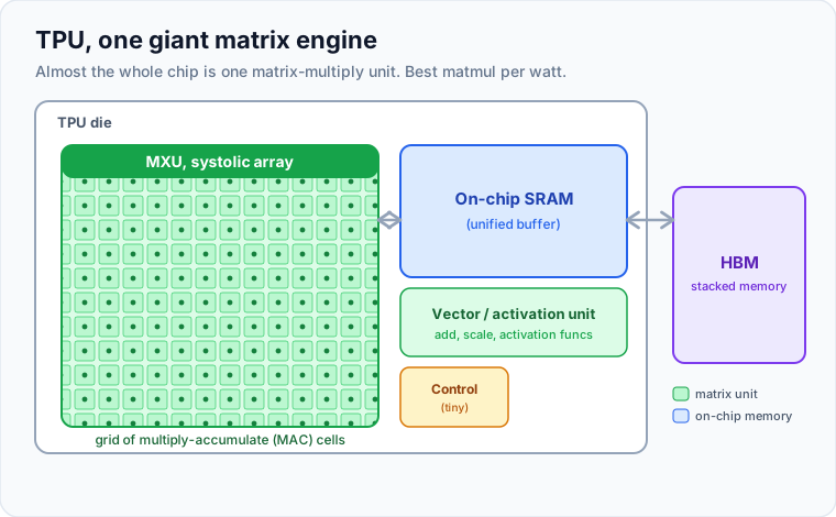
A TPU is an ASIC. It strips out the speculation, the big caches, and most control logic, and devotes the die to one systolic-array matrix unit (MXU) plus a large slab of on-chip SRAM. It does essentially one thing, big matrix multiplies and the element-wise ops around them, with exceptional performance per watt. The trade-off is flexibility: it shines on dense, predictable transformer/CNN math and is awkward for anything else.
Side by side
| Dimension | CPU 🧠 | GPU 🎛️ | TPU ⚙️ |
|---|---|---|---|
| Cores | A few powerful cores (~8 to 128) | Thousands of small cores (≈132 SMs on an H100) | One big systolic grid (e.g. 128×128 MACs) |
| Optimized for | Latency | Throughput | Matrix-multiply per watt |
| Parallelism | A few threads + SIMD | SIMT, massive data parallelism | Systolic dataflow |
| On-chip memory | Large caches (L1/L2/L3) | Registers + L1/shared + L2 | Big SRAM scratchpad |
| Main memory | DDR (~0.1 TB/s) | HBM / GDDR (~1 to 8 TB/s) | HBM (~1 to 3 TB/s) |
| Branchy/serial code | Excellent | Poor (divergence) | Not its job |
| Dense matmul | Modest | Excellent | Best per watt |
| Program with | C/C++, Python, SIMD | CUDA / ROCm / Triton | JAX / XLA, PyTorch-XLA |
| Flexibility | Highest | High | Low (matrix-shaped work) |
Rule of thumb: logic and control → CPU; parallel arithmetic → GPU; matrix multiplication at scale → TPU (or a GPU's tensor cores, next).
3. How Each One Runs Work
The divide above is really a divide in how work maps onto silicon.
- CPU (SIMD). A scalar stream that's superscalar (several instructions per cycle) and out-of-order, plus SIMD vectors (one instruction over 8 to 16 lanes). Real parallelism, but bounded.
- GPU (SIMT). You write code for one thread; the hardware runs them in warps of 32 in lockstep. Keep enough warps resident and memory latency disappears. The catch is divergence: if threads in a warp take different branches, the warp runs both sides with lanes masked off, which is why branchy code wastes a GPU.
- TPU (systolic). A grid of multiply-accumulate cells where weights stay put and data flows through, so each loaded value is reused across the whole array:
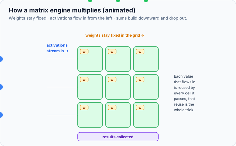
Animated: activations flow in from the left, cells compute in a wavefront, sums drop out the bottom.
| Model | Unit | Strength | Weakness |
|---|---|---|---|
| SIMD (CPU) | vector lanes | low latency, flexible | limited width |
| SIMT (GPU) | warps of 32 | massive parallelism, hides latency | branch divergence |
| Systolic (TPU) | 2D MAC grid | max operand reuse, perf/watt | matmul-shaped work only |
GPUs borrowed the systolic idea for their hottest path: a small matrix engine inside each SM. That's the tensor core.
4. Tensor Cores & Matrix Engines
Deep learning is, computationally, dense matrix multiplication (GEMM): linear layers are Y = XW, attention is a stack of matmuls, convolutions lower to matmuls. Make matmul fast and you make ML fast, and a scalar ALU is a wasteful way to do it.
A normal core does one multiply-add on two numbers. A tensor core multiplies two whole tiles and accumulates, in a single operation:
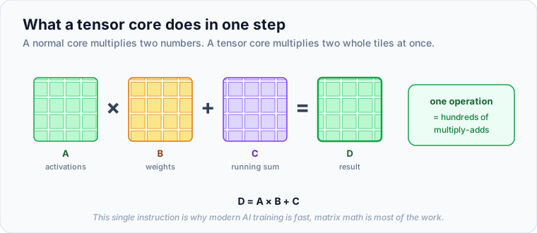
Because it performs and reuses an entire tile of multiply-adds at once, a tensor core delivers roughly an order of magnitude more matmul throughput than the same area of scalar cores. It is the single biggest reason modern training is feasible. Tensor cores have advanced mainly by adding lower-precision modes and tricks like 2:4 structured sparsity (skip half the weights for ~2× throughput):
| Generation (year) | Flagship | Tensor-core milestone |
|---|---|---|
| Volta (2017) | V100 | first tensor cores (FP16 with FP32 accumulate) |
| Ampere (2020) | A100 | TF32, BF16, and 2:4 sparsity |
| Hopper (2022) | H100 | FP8 + the Transformer Engine |
| Blackwell (2024) | B200 | FP4, second-gen Transformer Engine |
A TPU's MXU is the systolic equivalent, and other vendors ship matrix engines too (AMD Matrix Cores, Apple/Intel AMX).
Precision: the lever that made it fast. Fewer bits per number means more numbers per byte of bandwidth and more math per second, at some cost to accuracy. The art is using the least precision a workload tolerates:
| Format | Bits | Range | Typically used for |
|---|---|---|---|
| FP32 | 32 | wide | baseline; sensitive parts |
| TF32 | ~19 | FP32-like | default matmul math on Ampere+ |
| BF16 | 16 | FP32-like | training (preferred) |
| FP16 | 16 | narrow | training/inference (needs scaling) |
| FP8 | 8 | very narrow | Hopper+ training & inference |
| INT8 | 8 | quantized | fast inference |
The model still converges because products are accumulated in higher precision (FP32) inside the core; only the inputs are shrunk. (More on mixed precision in the PyTorch deep dive.)
5. GPU Memory: HBM, VRAM, Bandwidth
A tensor core is useless if it's starved for data. On modern accelerators, memory bandwidth, not FLOPs, is the bottleneck for a large share of real work. Memory lives in tiers: small and fast on top, big and slow below.
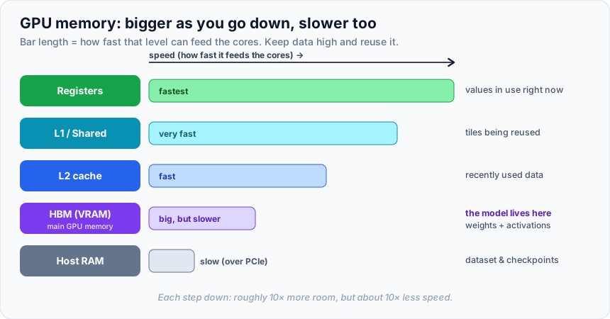
That big slab in the middle, HBM, is the GPU's main memory (its "VRAM"). It's fast because the DRAM dies are stacked vertically (connected by through-silicon vias) right next to the processor on a silicon interposer, giving an extremely wide bus of several TB/s, versus ~1 TB/s for the GDDR memory on consumer cards. HBM bandwidth is the headline spec on any AI accelerator, and the model plus everything it produces at runtime (activations, KV-cache) must fit inside it.
The key question for any kernel: is it waiting on math, or on memory?
📉 Memory-bound
Few FLOPs per byte loaded. The cores wait on HBM and tensor cores sit idle. A bigger chip won't help; you need bandwidth or more reuse.
📈 Compute-bound
Lots of FLOPs per byte loaded. The cores run flat out and the hardware is fully used. This is the happy place.
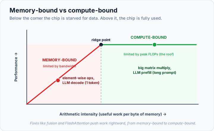
Engineers picture this with the roofline: performance climbs with arithmetic intensity (work per byte) until it hits the compute ceiling:
| Operation | Intensity | Usually |
|---|---|---|
| Element-wise (add, GeLU, scale) | low | memory-bound |
| LayerNorm / softmax | low | memory-bound |
| LLM decode (1 token) | low | memory-bound |
| Large dense GEMM | high | compute-bound |
| LLM prefill (long prompt) | high | compute-bound |
This explains the biggest wins in practice: kernel fusion and FlashAttention both raise arithmetic intensity, doing more math per trip to HBM, sliding work from the red zone into the green.
6. Talking Between Chips: Communication
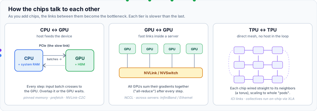
A single chip is never the whole story in real training. Data has to reach the GPU, and big models span many chips that must constantly share results. The moment you cross a chip boundary, the link becomes part of the memory hierarchy, and each step outward is dramatically slower:
| Link | Bandwidth | Scope |
|---|---|---|
| On-chip SRAM | ~10s of TB/s | within a chip |
| HBM | ~few TB/s | chip ↔ its own memory |
| NVLink / NVSwitch | ~100s GB/s to TB/s | GPU ↔ GPU within a server |
| PCIe | ~64 GB/s | host ↔ device |
| Network (IB/Ethernet) | ~25 to 400 Gb/s | server ↔ server |
The three communication patterns that matter in ML, side by side:
CPU ↔ GPU (host ↔ device)
In training, the CPU is the data engine: it reads, decodes, and augments each batch, then ships it to the GPU over PCIe, the slowest link in the box. It also loads model weights at startup, and with techniques like CPU/optimizer offload it can hold state that spills back and forth.
The risk is the GPU sitting idle waiting for data. The fixes are all about hiding that transfer: pinned (page-locked) memory for faster copies, prefetching the next batch while the current one trains, enough DataLoader workers to keep the queue full, and keeping tensors resident on the GPU instead of bouncing to the host. Newer designs shrink the gap with tighter coupling (NVLink-C2C in Grace Hopper).
GPU ↔ GPU
When a model is split across GPUs, they synchronize constantly. The workhorse operation is the all-reduce: every GPU sums its gradients with all the others so the model stays consistent. Often this runs as a ring: each GPU passes chunks to its neighbor until everyone holds the summed result:
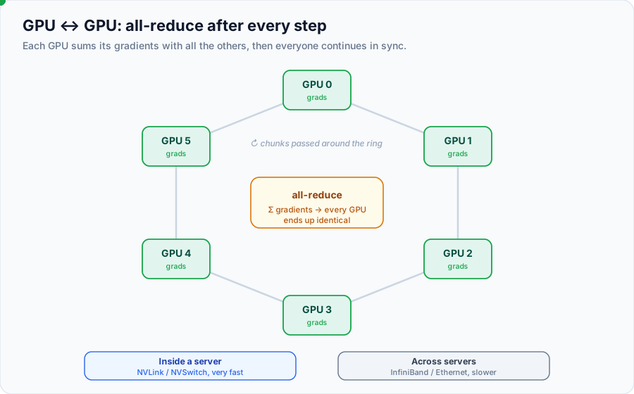
Inside a server this rides NVLink/NVSwitch (very fast); across servers it falls back to InfiniBand or Ethernet (much slower). The library that runs these collectives (all-reduce, all-gather, reduce-scatter) is NCCL, and the ring algorithm keeps bandwidth scaling as you add GPUs.
How you split the model decides how much they must talk:
| Strategy | Splits… | Main collective | Keep it… |
|---|---|---|---|
| Data parallel | the batch (model copies) | all-reduce gradients | anywhere (light-ish) |
| FSDP / ZeRO | weights + optimizer state | all-gather + reduce-scatter | within fast links |
| Tensor parallel | each layer's matmuls | per-layer, very heavy | within one server (NVLink) |
| Pipeline parallel | layers into stages | activations at borders | across servers (lighter) |
| Expert (MoE) | experts across devices | all-to-all routing | depends on routing |
The golden rule: put the chattiest parallelism (tensor) on the fastest links, and only split across slow server boundaries where the traffic is light. Mechanics of DDP and FSDP are in the PyTorch deep dive.
TPU ↔ TPU
TPUs are built to scale out. Each chip has dedicated ICI (Inter-Chip Interconnect) links wired directly to its neighbors in a 2D/3D torus, forming pods of thousands of chips. Two things stand out versus GPUs: the host (CPU) is not in the loop for chip-to-chip collectives, and the nearest-neighbor mesh is naturally efficient for all-reduce. The XLA compiler places the communication for you, so the same JAX/TF program scales from one chip to a full pod with little code change.
7. When to Use Each
🧠 Reach for a CPU
Orchestration and control planes, data prep/ETL, branchy or serial logic, small models, and low-traffic or latency-sensitive serving. Classical ML (trees, XGBoost) often runs fine here.
🎛️ Reach for a GPU
Training and research, mixed workloads, custom kernels (Triton), and most inference at scale. The flexible default for deep learning.
⚙️ Reach for a TPU
Very large, matmul-dominated training and inference at pod scale, especially on Google Cloud with the JAX/XLA stack. Strong cost-per-throughput for stable architectures.
| Workload | Best fit | Why |
|---|---|---|
| Data prep, ETL, glue code | CPU | branchy, I/O-bound, serial |
| Classical ML / small models | CPU | not matmul-heavy |
| Deep-learning training (research) | GPU | flexibility + CUDA ecosystem |
| Huge, stable, matmul-heavy training | TPU or GPU | TPU perf/watt vs GPU flexibility |
| High-throughput batched inference | GPU / TPU | tensor cores; batch → compute-bound |
| Low-latency single request | CPU or small GPU | latency dominates |
| Custom / dynamic-shape workloads | GPU | Triton/CUDA flexibility |
The real tie-breakers are usually software and availability, not raw speed: CUDA is the deepest, most portable ecosystem; TPUs live inside Google's stack.
8. It All Happens in One Training Step
Every idea above shows up in a single training step. Watch which part of the hardware each phase uses:
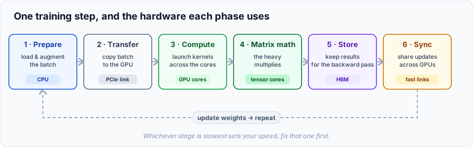
- The CPU prepares the next batch (decode, augment), branchy work it's good at.
- The batch crosses PCIe to the GPU. Overlap this with compute (prefetch) or it stalls everything.
- The GPU's cores launch kernels; warps are scheduled across SMs and occupancy hides HBM latency.
- Tensor cores do the forward and backward matmuls in BF16/FP8, where most FLOPs go.
- Activations sit in HBM; their size drives memory pressure (hence activation checkpointing).
- Across GPUs, gradients are summed over the fast links, the step the interconnect bounds.
Then weights update and it repeats. Tune the slowest stage, not everything.
9. Cheat Sheet
- CPU = latency, GPU = throughput, TPU = matrix math. It all follows from how transistors are spent.
- SIMT hides memory latency with parallelism: keep occupancy high and avoid warp divergence.
- Tensor cores multiply whole tiles at once, the reason modern training is feasible.
- Precision is a lever: BF16 for training, FP8/INT8 for inference, with high-precision accumulation.
- Memory bandwidth usually bounds real work, not compute. Classify memory- vs compute-bound first.
- HBM is the GPU's fast main memory; the model must fit in it. Links between chips are cliffs.
| If you're stuck on… | Try… |
|---|---|
| Branchy / serial code | run it on a CPU, not a GPU |
| Low GPU utilization | bigger batches; fuse kernels |
| Out of memory | lower precision; shard the model (FSDP) |
| Memory-bound kernel | do more math per memory trip (fusion, FlashAttention) |
| Slow data loading | more CPU workers; overlap the copy to GPU |
| Slow multi-GPU scaling | match parallelism to the link speeds |
10. References
- NVIDIA. NVIDIA H100 Tensor Core GPU Architecture (Hopper) Whitepaper. https://resources.nvidia.com/en-us-tensor-core
- NVIDIA. CUDA C++ Programming Guide (SIMT, warps, memory hierarchy). https://docs.nvidia.com/cuda/cuda-c-programming-guide/
- N. Jouppi et al. In-Datacenter Performance Analysis of a Tensor Processing Unit. ISCA 2017. https://arxiv.org/abs/1704.04760
- S. Williams, A. Waterman, D. Patterson. Roofline: An Insightful Visual Performance Model. CACM 2009. https://dl.acm.org/doi/10.1145/1498765.1498785
- T. Dao et al. FlashAttention: Fast and Memory-Efficient Exact Attention. NeurIPS 2022. https://arxiv.org/abs/2205.14135
- NVIDIA. Train With Mixed Precision (FP16/BF16/TF32/FP8). https://docs.nvidia.com/deeplearning/performance/mixed-precision-training/
- Google Cloud. TPU System Architecture (MXU, ICI, pods). https://cloud.google.com/tpu/docs/system-architecture-tpu-vm